This post is a research I did in my bachelors as a member of Ganesh-ICMC. I believe much of what I did there may be useful for more people, so I’d like to spread this knowledge through publications in this blog.
Last year I have discovered the book Open Circuits, from Eric Schlaepfer and Windell Oskay, and it had a collection of pictures from the inside of electronic components. The images are just beautiful and the photography technique is also very interesting. I always loved these images, so I follow many accounts on Twitter that post this kind of content, and it’s very nice to have the book as a collection of many things in one place.
But going further than the component’s beauty, it’s interesting to know how electronic circuits are built, how is the design process and how each component works. It’s possible to have even a quantitative notion of how certain components behave without going deep into electromagnetism principles.
In this post I’d like to discuss how Printed Circuit Boards (PBCs) and Integrated Circuits (ICs) are built, because they serve to connect different electronic components. I’d also like to go a little deep on how each of the basic components are built.
Printed Circuit Board Construction
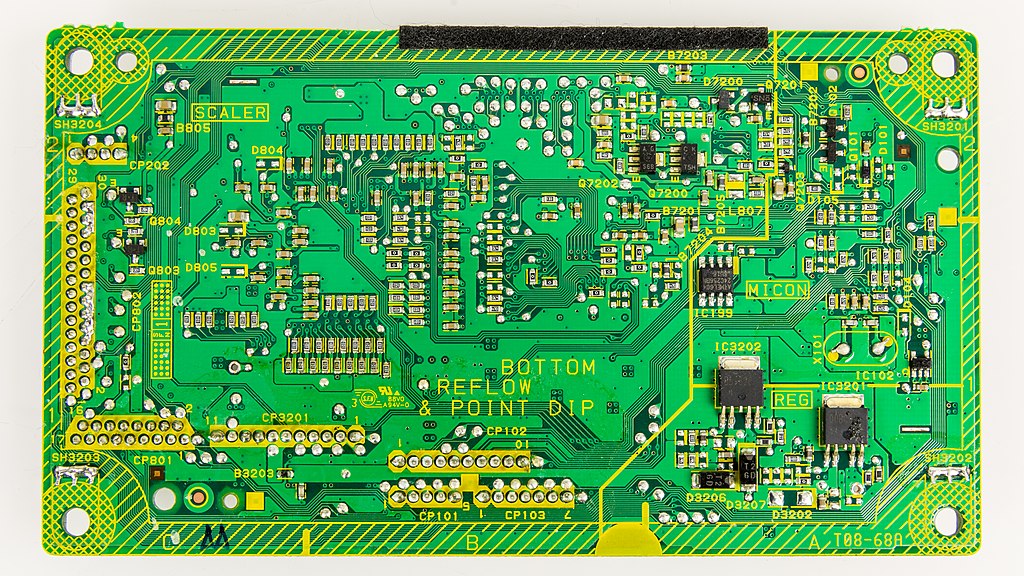
Anybody who had the curiosity to disassemble an electronic device may have seen a green board in which many electronic components were soldered in. These boards have the purpose of connecting the components and are called Printed Circuit Boards.
PCB from a television, by Raimond Spekking CC-BY-SA
A PCB is made of multiple copper trails divided by an insulator material, as shown in the figure below. The most common insulator material is the FR-4 (Flame Retardant), which tries to minimize the risk of electrical sparks. But other applications may use other materials, like Roger’s dielectric for microwave circuits and the polyethylene plastic for flexible PCBs.
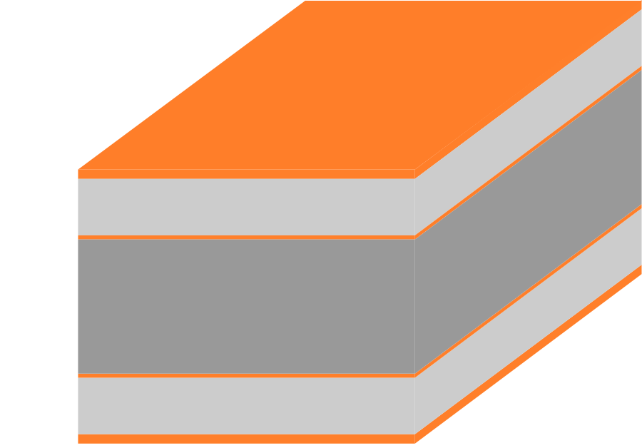
Different layers of a PBC
These cooper layers can be connected through vias, which basically are cooper tubes connecting two layers. These vias can pass through the whole PCB (1. Through hole), which is necessary to solder components whose pins go through the board. The vias can also start from the surface and stop at an internal layer (2. Blind via) or even connect two internal layers (3. Buried via).
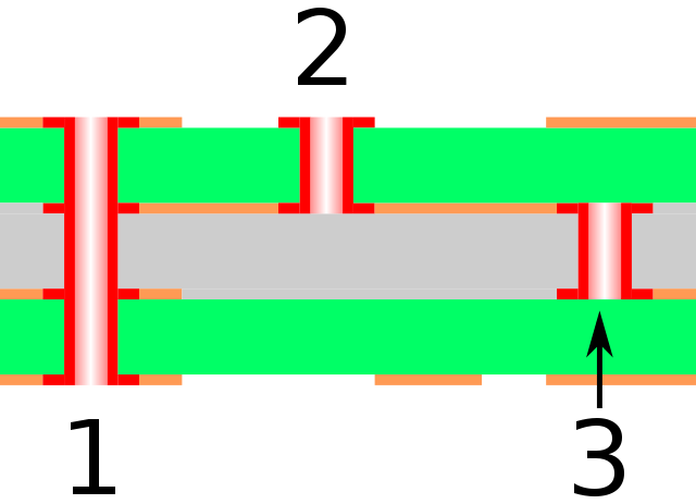
Different types of vias, by M adler CC-BY
Observe that the internal cooper layers and the buried vias are impossible to see with the naked eye, but they can still be observed through X-ray imaging.
Once the PCB manufacturing is done, the circuit is finished by soldering the components. These components can be soldered using pins that perforate the PCB, and are called Plated Through Hole (PTH) components, or they can just lie on the board, and be called Surface Mounted Device (SMD). There is a preference for SMD devices because they can be soldered mechanically through pick-and-place machines, while PTH components are soldered by hand.
The figure below shows a simple example board with both types of components. The IC marked as “U1” and the transistor marked as “Q1” are SMD, all other components are PTH.
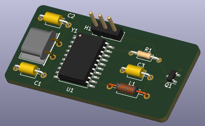
Example PCB with all components set
Once the components are soldered, the circuit is ready for use.
Integrated Circuit Construction
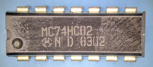
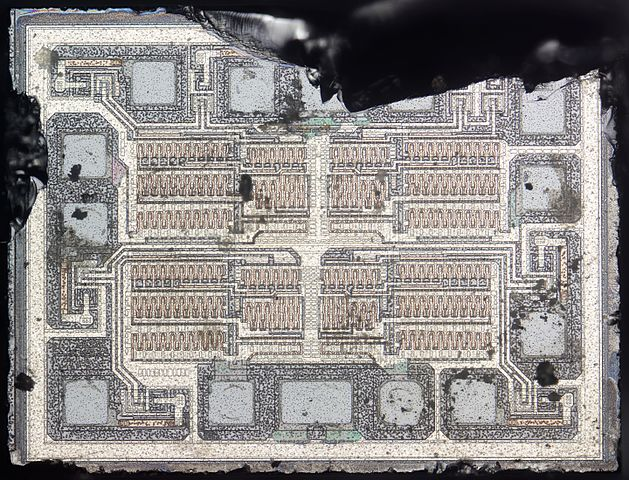
Integrated Circuits are based in semiconductor materials and usually show up in PCBs inside a rectangular black package. Their use in electronics is very important because they are able to build digital circuits, like microprocessors. The figure below shows a simple digital circuit containing four NOR logic gates with 2 inputs.
Packaging and the chip inside it, by Robert Baruch CC-BY-SA
Its structure is similar to a PCB, electronic components like diodes and transistors are developed at the semiconductor material substrate and are connected by metal structures. There structures are different metal layers connected by vias, just as in PCBs, and are immersed in an insulating material.
In terms of materials, the semiconductor substrate is usually silicon; the metal layers cooper or aluminum; the vias tungsten; and the insulator silicon oxide.
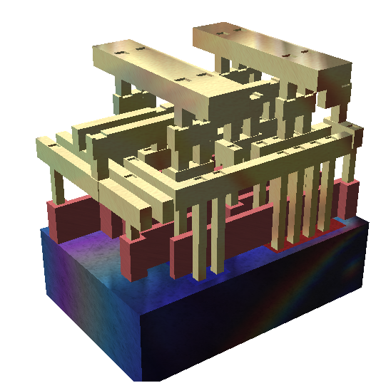
The figure below shows a 3D representation of an integrated circuit section. The base with a rainbow pattern is the silicon substrate and the yellow structures are metal. On the substrate there are light red structures which are transistor’s gates and there are red and blue regions at the subtrate that represent silicon with P and N doping, but to understand better how this works we will go in more detail on howo a transistor works in the section about components.
3D integrated circuit, by David Carron CC0
Design Process
The design process of PCBs and ICs aims to define what patterns should be transferred to each layer the manufacturing process can control, that is: what shape should the metal layer have, where should the vias be, what silicon regions should be doped, etc.
The design process for PCBs and ICs are basically the same. The project starts with a schematic, which defines what are the used components and how they should connect. Then a layout is made, in which each of the schematic component is mapped to the shape that should actually be drawn, the component’s footprint, and the designer decides about their placement and draws their connections.
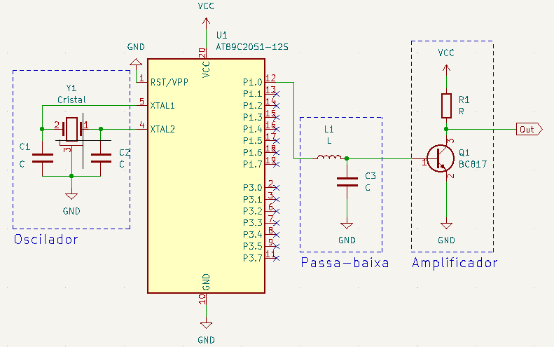
Schematic of the example circuit
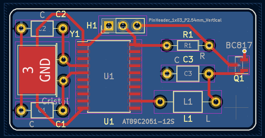
Layout developed from the schematic
In the schematic’s figure, each component has brown color and the connections are green lines.
In the layout figure, there are two cooper layers, being the front layer represented in red and the back one in blue. The yellow circles represent vias, and the silkscreen writings show up in light yellow.
Using the annotated name for each component like “U1” and “R1”, we can observe the mapping of each component from the schematic to its shape in the layout.
Finally, the layout can be sent to manufacturing so that a board like the one in the figure below can be made.
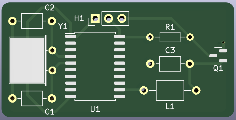
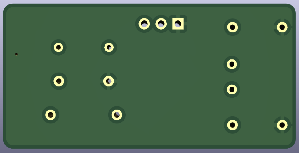
Top and bottom view of the example PCB
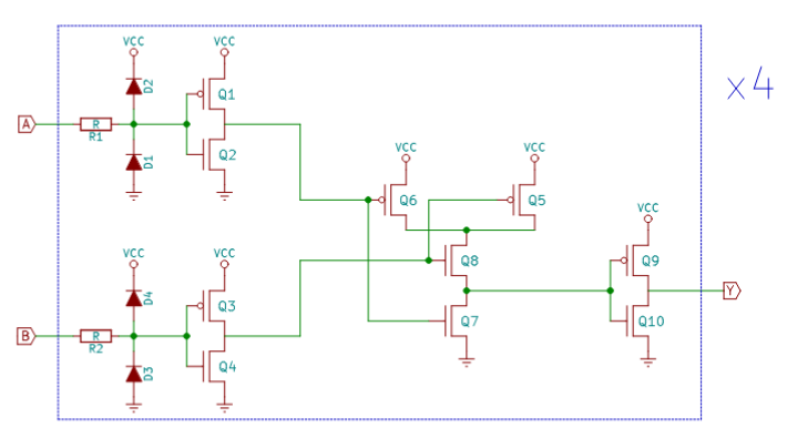
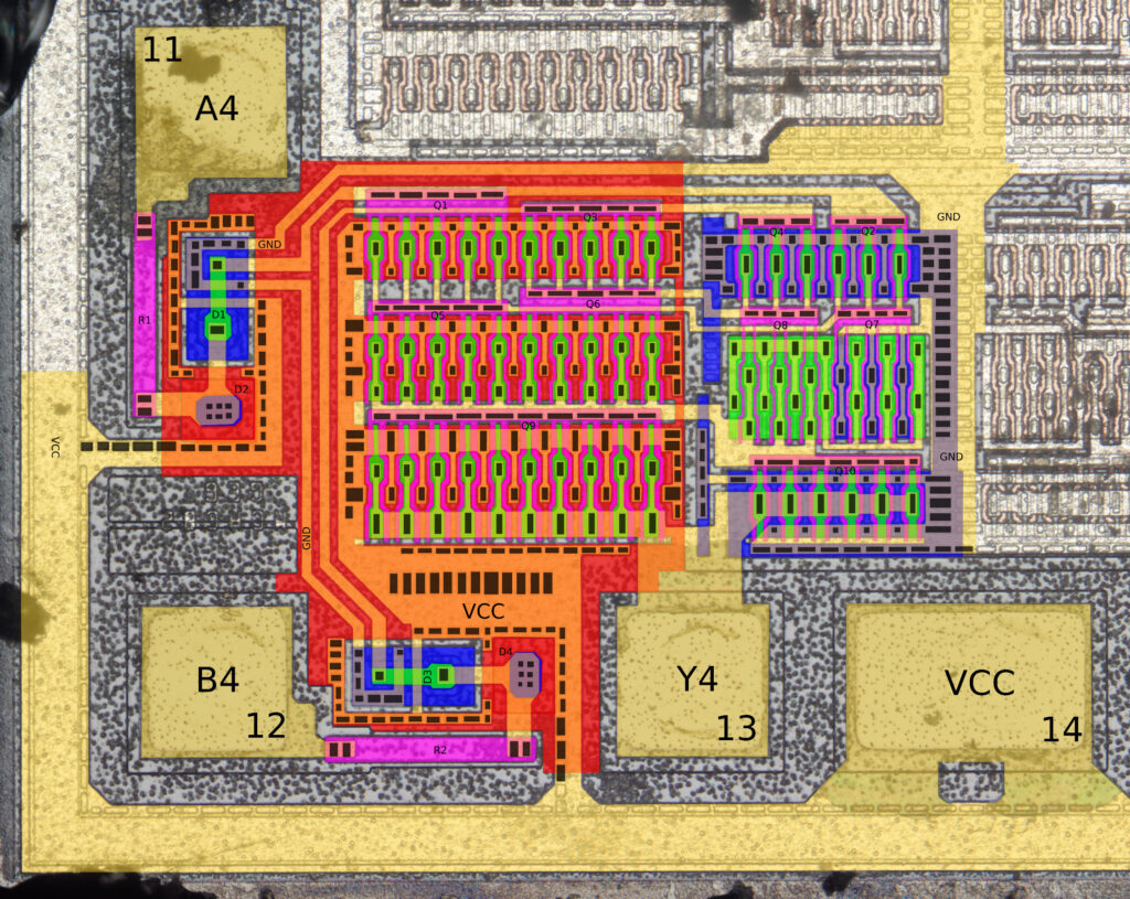
And down below there is an schematic and a layout of an integrated circuit, being the procedure basically the same. In this case both were obtained through reverse engineering.
IC Schematic, by Robert Baruch CC-BY-SA
IC layout, by Robert Baruch CC-BY-SA
In the figure it’s possible to identify some of the components. From the input pad B4, we can see the signal passes through a resistor highlighted in pink, and then by two other structures, which are diodes. Then the signal goes through a sequence of transistors until it gets to the the Y4 output pad.
Basic components
RESISTOR:
A resistor basically dissipates energy in the form of heat and can be used to control voltages and currents. Its behavior is described by the first Ohm’s law, which proposes the current that passes through a resistor is proportional to the voltage applied to it, being the resistance value the ratio between the voltage and the current.
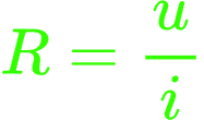
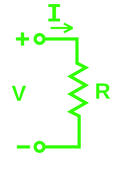
In the equation “R” is the resistance, “u” is the voltage and “i” is the current.
Physically, the resistance of a wire with uniform cross-sectional are and material can be described by the second Ohm’s law, which proposes that the thinnest and the longest a wire is, the bigger is its resistance.
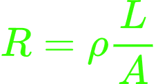
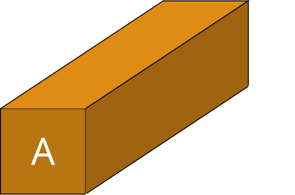
In the equation, “R” is the resistance, “ρ” is the material’s resistivity, “L” is the wire length and “A” is the cross-sectional area.
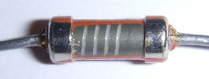
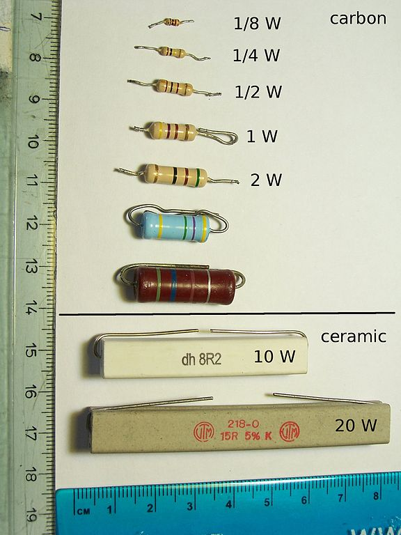
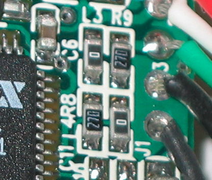
Then it’s possible to build a resistor with a desired value taking a conducting material with known resistivity and choosing an adequate length and thickness. The images below show examples of resistors that are commonly used in PCBs:
CAPACITOR:
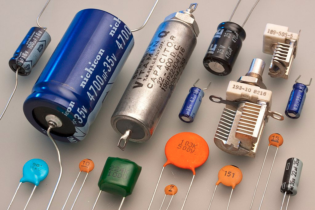
A capacitor stores energy in the form of an electric field and can be used to store energy and stabilize voltages. Its behavior is described by the current equation for capacitors, which says that the current is proportional to variations of voltage on time, being the capacitance value the ratio between the current and the variation intensity. This equation also proposes that when the voltage is constants (like after a DC circuit stabilizes) there is no current through the capacitor, so it behaves like an open circuit.
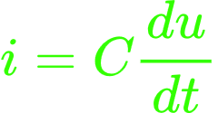
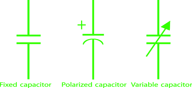
In the equation “i” is the current, “C” is the capacitance, “u” is the voltage and “t” is time.
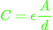
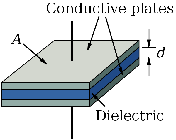
Physically, we can determine the capacitance of two parallel conducting plates by the equation below. It tells that the biggest the plate’s areas and the smallest the distance between them, the biggest is the capacitance. Also, it’s important to notice the capacitance depends only on the isolating material electrical permittivity and not on the conducting material.
In the equation, “C” is capacitance, “ε” is the isolating material electric permittivity, “A” is each plate’s area and “d’ the is the distance between them.
With this, it’s possible to build a capacitor from a thin foil of insulating material covered on both sides by a layer of conducting material. The image below show examples of capacitors used in PCBs.
Different types of capacitors, by Eric Schrader CC-BY-SA
INDUCTOR:
An inductor stores energy in the form of a magnetic field and can also be used to store energy and stabilize currents. Its behavior is described by the equation of voltage in the inductor, which proposes that the voltage in the inductor’s terminals is proportional to the change of current inside it, being the inductance value the ratio between the voltage and the current variation in time. The equation also shows that when the current is constant, the voltage is zero, so the inductor behaves as a short-circuit.
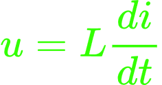

Inductor symbol
In the equation “u” is the voltage, “L” is the inductance, “i” is the current and “t” is time.
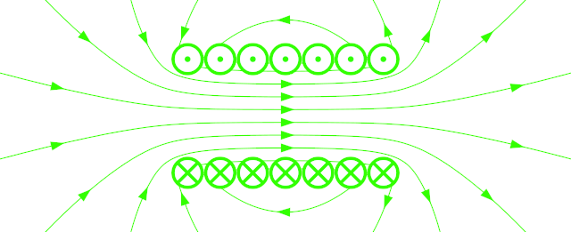
Physically, we can determine the inductance of a solenoid (basically a wounded wire) through the equation below. It states that the biggest the area covered, the spin density and the length, the biggest is the inductance.

Solenoid diagram, by geek3 CC-BY-SA
In the equation, “L” is inductance, “μ” is the magnetic permeability inside the solenoid, “n” is the number of spins by length, “l” is the solenoid’s length (not the wire length), and “A” is the cross-sectional area.
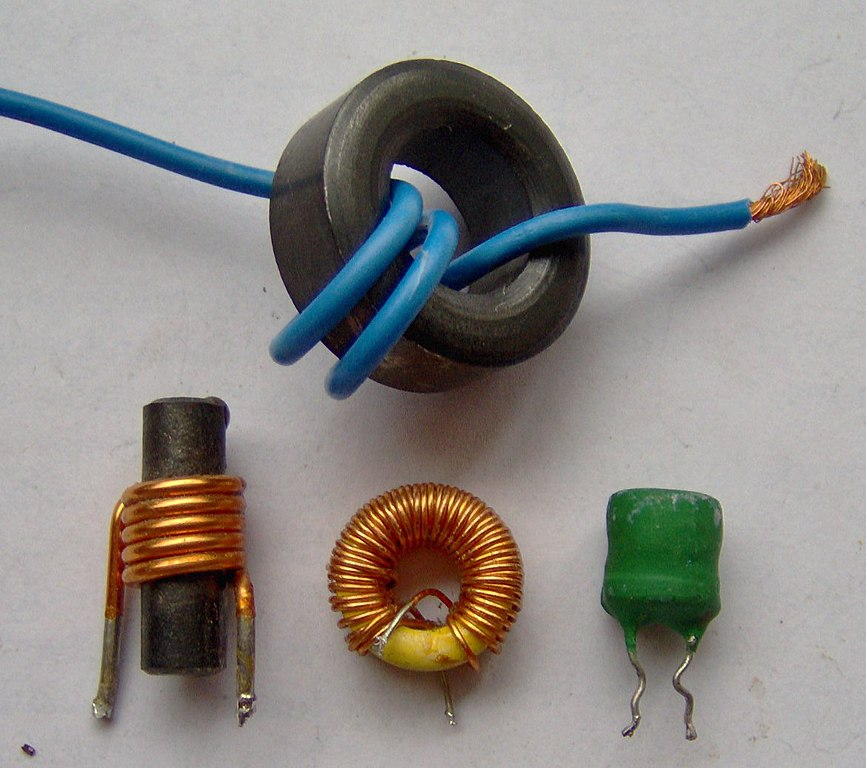
With this, it’s possible to build an inductor using a conducting wire (covered by an isolating material to avoid shorts) wounded, preferably, around a metallic core to maximiza the magnetic permeability. The image below shows examples of inductors used in PCBs.
Different inductors, by Miguel CC-BY-SA
DIODE:
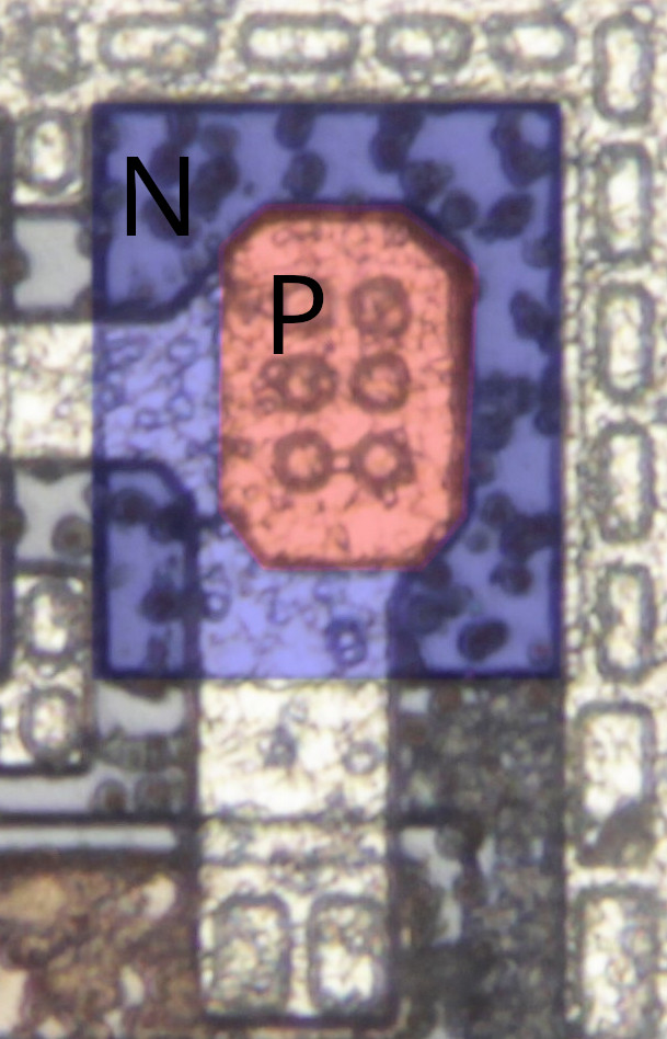
Contrary to the previous components, diodes and transistores are based in semiconductor materials, and are build from doping, a process that adds a small impurity in the semiconductor to change its electrical properties. How semiconductor physics work is beyond the scope of this article, but there are two types of doping: P type, in which the impurity creates positive free charges, or N type, in which the impurity creates negative free charges.
A diode, in brief, allows for the passage of current in one direction, but blocks the opposite one. Their physical construction is based in semiconductor materials and consists on the junction of a P-doped region with an N-doped region, the P-N junction. Its symbol points to the direction the current can pass.
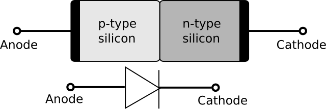
Diode’s P-N junction and its symbol, by Raffamaiden CC-BY-SA
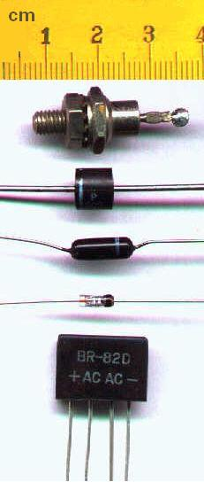
For PCB design, one can use discrete diodes, as in the left figure, but in IC design it’s possible to build diodes directly in the silicon substrate, as shown in the right figure.
Different discrete diodes, by Ulfbastel CC-BY-SA
Diode inside an IC, by Robert Baruch CC-BY-SA (crop and color from me)
TRANSISTOR:
A transistor, in brief, is a controlled switch. In the case of MOSFET (Metal Oxide Semiconductor Field Effect Transistor) transistors, the source and drain terminals can be either shorted or disconnected depending on the voltage applied to the gate. For the NMOS, the transistor is shorted when the gate voltage is in high logic level and the PMOS is shorted at low logic level.
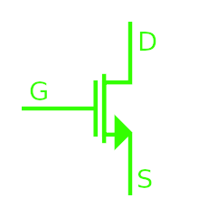
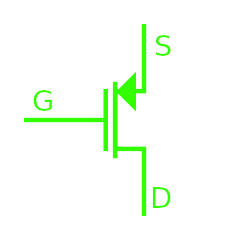
The image below shows the physical structure of an NMOS transistor. There the source and drain consist of N-doped regions separated by a P-doped region.
This doping configuration N, P and N, in principle blocks the passage of current, because it’s equivalent to two back-to-back diodes and blocks current in both directions. However, the gate terminal can create an inversion of the P substrate and create a channel equivalent to an N doping, so the source and drain are directly connected.

Side view of a NMOS transistor, by Olivier Deleage and Peter Scott CC-BY-SA
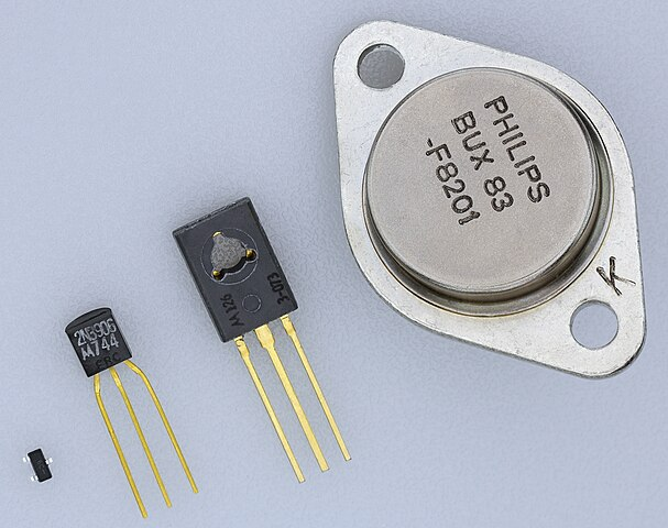
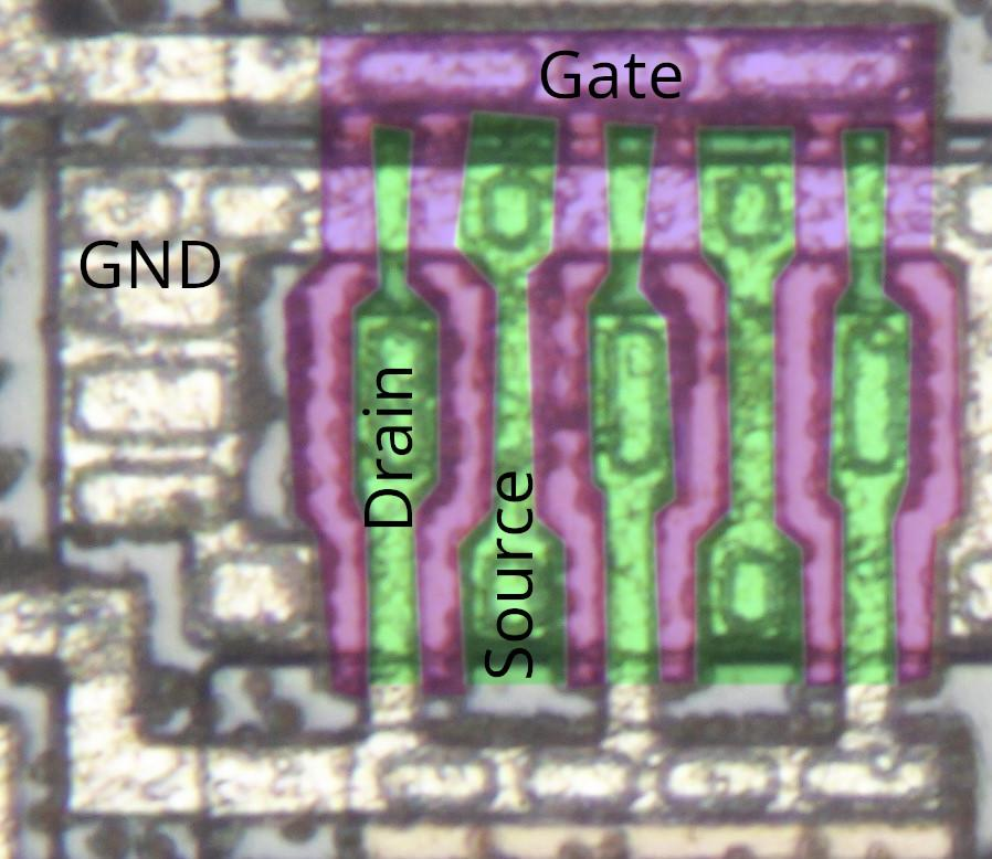
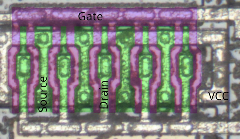
As in the diode’s case, transistors can be used as discrete components in PCBs or directly built in the IC’s silicon substrate, as shown in the images below.
Different types of transistors, by Mister rf CC-BY-SA
NMOS transistor inside an IC, por Robert Baruch CC-BY-SA (crop and color from me)
PMOS transistor inside an IC, por Robert Baruch CC-BY-SA (crop and color from me)
Discussion
With this post I hope to have satisfied the curiosity of those who want to understand on a deeper level how an electric circuit is built, exploring each component and how they connect. From this notion I hope the reverse engineering of hardware becomes a less obscure process.
There more to explore beyond the components mentioned here, and in high-frequency circuits, certain components can show up as patterns drawn to the board instead of a discrete component. A power divider, for example, is two trails passing close one from the other. And distributed element circuits allow for the construction of complete filters using only patterns drawn to the board.
1 Comment
Hey people!!!!!
Good mood and good luck to everyone!!!!!